Difference between revisions of "DDR3-CycloneV interface description"
m (→Downloads) |
(→General description) |
||
| Line 32: | Line 32: | ||
== General description == | == General description == | ||
| − | + | ||
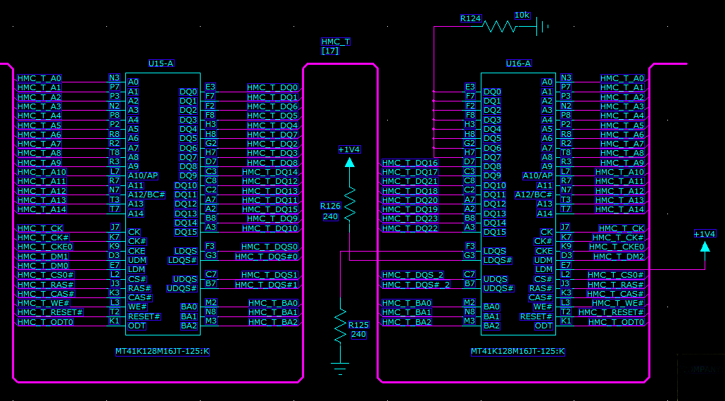
Diagram below describe the connections between the CycloneV and the two DDR3 blocks. Each DDR3 blocks has two banks of 128MB, on one chip (U15) all data are used, and on the other chip, only 128MB are used, the second bank is not plugged. Thus, the amount of ram accessible via the fpga is 384MB, with a data bus of 24bits. | Diagram below describe the connections between the CycloneV and the two DDR3 blocks. Each DDR3 blocks has two banks of 128MB, on one chip (U15) all data are used, and on the other chip, only 128MB are used, the second bank is not plugged. Thus, the amount of ram accessible via the fpga is 384MB, with a data bus of 24bits. | ||
Revision as of 17:22, 2 February 2016
Contents
Introduction
2 RAMs are connected to CycloneV's APF6_SP.
Parameters
- DDR3:
| part | MT41K128M16JT-125 |
| type | DDR3L |
| Speed | 750Mhz |
| timings | See verilog model provided by micron |
| JEDEC | JEDEC DDR3-1600 -> JEDEC DDR3-1G6 2GB x8 |
| Chip size | 2048Mbits -> 128M x 16bits |
General description
Diagram below describe the connections between the CycloneV and the two DDR3 blocks. Each DDR3 blocks has two banks of 128MB, on one chip (U15) all data are used, and on the other chip, only 128MB are used, the second bank is not plugged. Thus, the amount of ram accessible via the fpga is 384MB, with a data bus of 24bits.
To use the DDR3 SDRAM Controller with UniPhy provided by Quartus to instanciate the DDR3. See above how to do with Qsys.
How to integrate DDR3 chips in Qsys
UniPhy Howto
This is a click howto configure the DDR3 controller in the APF6_SP.
- Once the quartus project open, select your device correctly (see the product page to now the exact part name).
- In the IP Catalog, select :
installed IP->Library->Memory interfaces and Controllers->Memory Interfaces with UniPHY->DDR3 SDRAM Controller with UniPhy
- In the right frame select :
JEDEC DDR3-1G6 2GB x8
- Then click on Apply
- Select checkbox Enable Hard External Memory Interface (above the 6 configs tab).
- Tab PHY Settings:
- Speed grade : 8
- Memory clock frequency : 375Mhz
- PLL reference clock frequency : 62.5 Mhz
- Rate on Avalon-MM Interface : Full
- Supply voltage : 1.35V DDR3L
- Tab Memory parameters
- Memory device speed grade : 400Mhz
- Total interface width : 24
- Row address width : 14
- Tab Controller Settings (Optionnal if you wan't to use the two DDR3 chip)
- Select checkbox Expand Avalon-MM data for ECC
- Select 48bits instead of 32
- Finish
| |
Note: Using 48bits instead 32 is not standard for avalon it can be harder to connect inside your design |
Clock
The hard controller IP «DDR3 SDRAM Controller with UniPHY» require using and external oscillator to clock it. On APF6_SP, the all CycloneV fpga is clocked with the PCIe clock at 62.5Mhz by default.
To force Quartus to use the coreclkout as input clock for DDR3 controller a little hack must be done after HDL code is generated.
The DDR3 clock hack
| |
Note: If you include the .qsys under your Quartus project, Quartus will regenerate all the Qsys HDL/TCL code each times you synthesize your design, and will erase the modification. |
- Generate the design with Qsys
- Connect the pll_ref_clk of IP DDR3 SDRAM Controller with UniPHY on coreclkout of Avalon-MM Cyclone V Hard IP for PCI Express.
- Do all connections you need/want
- Generate the HDL code with Finish button.
- Under Quartus include the file your_project.qip and not your_project.qsys
- Find the file named *_p0_pin_map.tcl :
$ find . -name "*_p0_pin_map.tcl"
- It must be under directory named your_project/synthesis/submodules/
- Edit it and looking for line begining with :
proc YOUR_PROJECT_NAME_mem_if_ddr3_emif_0_p0_get_input_clk_id { pll_output_node_id } {
- Add this line at the begining of function :
return $pll_output_node_id
- Then synthesize all.
- Find the file named *_p0_pin_map.tcl :
| |
Note: In one line :$ find . -name "*_p0_pin_map.tcl" | xargs sed -iolt "/_mem_if_ddr3_emif_0_p0_get_input_clk_id {/a return \$pll_output_node_id"
|
IO
Downloads
Soon here, some examples project to downloads.

