Difference between revisions of "OPOS6UL SP Interfaces description"
(→Pinout) |
(→Simplified view) |
||
| Line 10: | Line 10: | ||
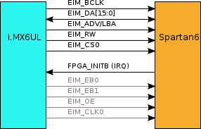
This article describe the bus interface communication between the i.MX6UL(L) and the spartan6. In i.MX6UL(L) the bus used to make communication with the FPGA is named '''EIM''' for '''E'''xternal '''I'''nterface '''M'''odule. All description of this bus can be found under the i.MX6UL(L) reference manual in chapter 21 (page 821). | This article describe the bus interface communication between the i.MX6UL(L) and the spartan6. In i.MX6UL(L) the bus used to make communication with the FPGA is named '''EIM''' for '''E'''xternal '''I'''nterface '''M'''odule. All description of this bus can be found under the i.MX6UL(L) reference manual in chapter 21 (page 821). | ||
| + | |||
== Simplified view == | == Simplified view == | ||
| + | |||
| + | [[File:OPOS6UL_SP_EIM_FPGA_INTERFACE.svg]] | ||
== Default configuration on CSx == | == Default configuration on CSx == | ||
Revision as of 15:57, 26 April 2019
Page under construction...
 Informations on this page are not guaranteed !!
Contents
Introduction
This article describe the bus interface communication between the i.MX6UL(L) and the spartan6. In i.MX6UL(L) the bus used to make communication with the FPGA is named EIM for External Interface Module. All description of this bus can be found under the i.MX6UL(L) reference manual in chapter 21 (page 821).
Simplified view
Default configuration on CSx
Clocks
The clock used to clock the FPGA is EIM_BCLK (IO_L1P_CCLK_2(N12) and IO_L29P_GCLK3_2(N8)) and is configured to 99 MHz.
Chip Select
The EIM memory space is mapped into 128 MB total memory space in the processor memory. This memory space begin at address 0x50000000
| Start address | End address | Size | Name |
|---|---|---|---|
| 0x5000_0000 | 0x57FF_FFFF | 128 MB | EIM (NOR/SRAM) |
The total 128 MB of memory can be divided among the EIM four chip selects. See reference manual of i.MX6ULL for more information.
Timings
HDL register access examples
Pinout
UCF example for interface generated by POD is given here :
NET "rstgen_syscon00_ext_clk" LOC="N8" | IOSTANDARD=LVCMOS33; # EIM_BCLK
NET "rstgen_syscon00_ext_clk" TNM_NET = "rstgen_syscon00_ext_clk";
TIMESPEC "TS_rstgen_syscon00_ext_clk" = PERIOD "rstgen_syscon00_ext_clk" 10.101 ns HIGH 50 %;
NET "imx6ul_wb16_wrapper00_imx_da<0>" LOC="P11" | IOSTANDARD=LVCMOS33; # EIM_DA0
NET "imx6ul_wb16_wrapper00_imx_cs_n" LOC="R11" | IOSTANDARD=LVCMOS33; # EIM_CS0
NET "imx6ul_wb16_wrapper00_imx_da<1>" LOC="M11" | IOSTANDARD=LVCMOS33; # EIM_DA1
NET "imx6ul_wb16_wrapper00_imx_da<2>" LOC="N11" | IOSTANDARD=LVCMOS33; # EIM_DA2
NET "imx6ul_wb16_wrapper00_imx_da<10>" LOC="R10" | IOSTANDARD=LVCMOS33; # EIM_DA10
NET "imx6ul_wb16_wrapper00_imx_da<11>" LOC="L9" | IOSTANDARD=LVCMOS33; # EIM_DA11
NET "imx6ul_wb16_wrapper00_imx_da<12>" LOC="M10" | IOSTANDARD=LVCMOS33; # EIM_DA12
NET "imx6ul_wb16_wrapper00_imx_da<13>" LOC="M8" | IOSTANDARD=LVCMOS33; # EIM_DA13
NET "imx6ul_wb16_wrapper00_imx_da<14>" LOC="K8" | IOSTANDARD=LVCMOS33; # EIM_DA14
NET "imx6ul_wb16_wrapper00_imx_da<15>" LOC="L8" | IOSTANDARD=LVCMOS33; # EIM_DA15
NET "imx6ul_wb16_wrapper00_imx_adv" LOC="R7" | IOSTANDARD=LVCMOS33; # EIM_LBA
NET "imx6ul_wb16_wrapper00_imx_da<7>" LOC="N6" | IOSTANDARD=LVCMOS33; # EIM_DA7
NET "imx6ul_wb16_wrapper00_imx_rw" LOC="R6" | IOSTANDARD=LVCMOS33; # EIM_RW
NET "imx6ul_wb16_wrapper00_imx_da<3>" LOC="P5" | IOSTANDARD=LVCMOS33; # EIM_DA3
NET "imx6ul_wb16_wrapper00_imx_da<4>" LOC="R5" | IOSTANDARD=LVCMOS33; # EIM_DA4
NET "imx6ul_wb16_wrapper00_imx_da<5>" LOC="L6" | IOSTANDARD=LVCMOS33; # EIM_DA5
NET "imx6ul_wb16_wrapper00_imx_da<6>" LOC="L5" | IOSTANDARD=LVCMOS33; # EIM_DA6
NET "imx6ul_wb16_wrapper00_imx_da<8>" LOC="M5" | IOSTANDARD=LVCMOS33; # EIM_DA8
NET "imx6ul_wb16_wrapper00_imx_da<9>" LOC="N5" | IOSTANDARD=LVCMOS33; # EIM_DA9
NET "irq_mngr00_gls_irq" LOC="P3" | IOSTANDARD=LVCMOS33; # FPGA_INITB
FPGA Interrupt
FPGA configuration protocol
Links
- i.MX6UL(L) reference manual (PDF chapter 21 page 821)
- i.MX6UL(L) Datasheet (PDF)
- Spartan6 configuration (PDF)
- Peripheral On Demand configuration files
